本文包含原理图、PCB、源代码、封装库、中英文PDF等资源
您需要 登录 才可以下载或查看,没有账号?注册会员
×
Freescale 公司的MC9S08LL16 是8位段LCD 微控制器,高达20MHz的CPU,工作电压3.6V-1.8V,工作温度-40℃到85℃. MC9S08LL16支持多达32个中断源/重置源,主要用在手提医疗设备,个人诊断,以电池为能源的设备,低端计量表,带显示的ZigBee节点,小型家电等.本文介绍MC9S08LL16主要特性,方框图以及演示板DEMO9S08LL16主要特性和详细电路图.
S08LL 8-bit segment LCD microcontroller family is ideal for battery-powered applications such as medical diagnostics or handheld appliances. The S08LL family extends battery life with industry leading low-power technology, eases development time and eliminates any excess cost with its complete Tower ecosystem.
MC9S08LL16主要特性:
· 8-Bit HCS08 Central Processor Unit (CPU)
– Up to 20-MHz CPU at 3.6V to 1.8V across temperature range of -40℃ to 85℃
– HC08 instruction set with added BGND instruction
– Support for up to 32 interrupt/reset sources
· On-Chip Memory
– Dual Array FLASH read/program/erase over full operating voltage and temperature
– Random-access memory (RAM)
– Security circuitry to prevent unauthorized access to RAM and FLASH contents
· Power-Saving Modes
– Two low power stop modes
– Reduced power wait mode
– Low power run and wait modes allow peripherals to run while voltage regulator is in standby
– Peripheral clock gating register can disable clocks to unused modules, thereby reducing currents.
– Very low power external oscillator that can be used in stop2 or stop3 modes to provide accurate clock source to real time counter
– 6 usec typical wake up time from stop3 mode
· Clock Source Options
– Oscillator (XOSC) - Loop-control Pierce oscillator; Crystal or ceramic resonator range of 31.25 kHz to 38.4 kHz or 1 MHz to 16 MHz
– Internal Clock Source (ICS) - Internal clock source module containing a frequency-locked-loop (FLL) controlled by internal or external reference; precision trimming of internal reference allows 0.2% resolution and 2% deviation over temperature and voltage; supports bus frequencies from 1MHz to 10 MHz.
· System Protection
– Watchdog computer operating properly (COP) reset with option to run from dedicated 1-kHz internal clock source or bus clock
– Low-Voltage Warning with interrupt
– Low-Voltage Detection with reset or interrupt
– Illegal opcode and illegal address detection with reset
– Flash block protection
· Development Support
– Single-wire background debug interface
– Breakpoint capability to allow single breakpoint setting during in-circuit debugging (plus two more breakpoints in on-chip debug module)
– On-chip in-circuit emulator (ICE) debug module containing three comparators and nine trigger modes. Eight deep FIFO for storing change-of-flow addresses and event-only data. Debug module supports both tag and force breakpoints
· Peripherals
– LCD - 4x28 or 8x24 LCD driver with internal charge pump and option to provide an internally regulated LCD reference that can be trimmed for contrast control.
– ADC - 8-channel, 12-bit resolution; 2.5 μs conversion time; automatic compare function; temperature sensor; internal bandgap reference channel; operation in stop3; fully functional from 3.6V to 1.8V
– ACMP - Analog comparator with selectable interrupt on rising, falling, or either edge of comparator output; compare option to fixed internal bandgap reference voltage; outputs can be optionally routed to TPM module; operation in stop3
– SCI - Full duplex non-return to zero (NRZ); LINmasterextended break generation; LIN slave extended break detection; wake up on active edge
– SPI- Full-duplex or single-wire bidirectional; Double-buffered transmit and receive;masteror Slave mode; MSB-first or LSB-first shifting
– IIC - IIC with up to 100 kbps with maximum bus loading; Multi.masteroperation; Programmable slave address; Interrupt driven byte-by-byte data transfer; supports broadcast mode and 10-bit addressing
– TPMx - Two 2-channel (TPM1 and TPM2); Selectable input capture, output compare, or buffered edge- or center-aligned PWM on each channel;
– TOD- (Time Of Day) 8-bit quarter second counter with match register; External clock source for precise time base, time-of-day, calendar or task scheduling functions; Free
running on-chip low power oscillator (1 kHz) for cyclic wake-up without external components.
· Input/Output
– 38 GPIOs, 2 output-only pins
– 8 KBI interrupts with selectable polarity
– Hysteresis and configurable pull up device on all input pins; Configurable slew rate and drive strength on all output pins.
· Package Options 64-LQFP, 48-LQFP and 48-QFN
MC9S08LL16目标应用:
Battery powered applications
Portable medical devices
Thermostats
AlARMs/clocks
Exercise equipment
Personal diagnostics
Calculators
Low-end utility metering
ZigBee® nodes with display
Scrolling text displays
Small appliances
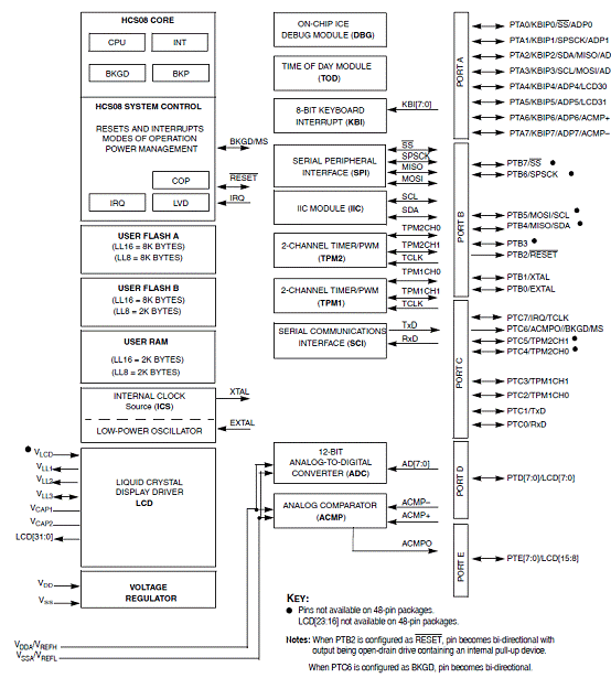
图1.MC9S08LL16 系列方框图
MC9S08LL16 演示板DEMO9S08LL16
The DEMO9S08LL16 is a demonstration board for the MC9S08LL16 microcontroller. Application development is quick and easy with the integrated USB-BDM, sample software tools, and examples. An optional BDM_PORT port is also provided to allow use of a BDM_PORT cable. Two, 40-pin connectors provide access to all IO signals on the target MCU.
The cost effective DEMO9S08LL16 demonstration kit contains everything a designer needs to develop and evaluate application code. The integrated USB multilink allows a designer to communicate with the board and target device with only a USB cable
演示板DEMO9S08LL16主要特性:
MC9S08LL16, 64 LQFP
Integrated P&E USB-BDM
On-board +5V regulator
Battery holder for Li-ion battery
Power Input Selection Jumpers
5 Push Switches; 4 User, 1 Reset
10 LED Indicators; 8 User, VDD, USB
5K ohm POTs w /LP Filter
Light Sensor w/ LP Filter and Op Amp
User Option Jumpers to disconnect Peripherals
40-pin MCU I/O Connector
2.0mm Barrel Connector
BDM_PORT (not installed)
USB Connector
DB9 Connector
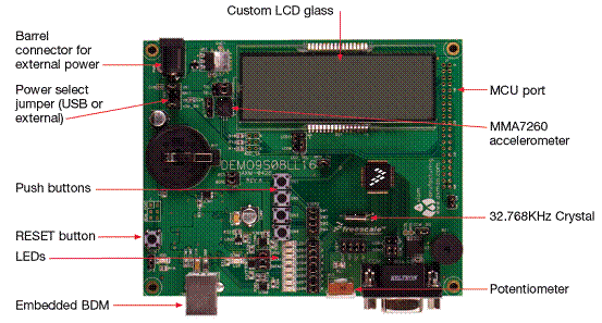
图2.演示板DEMO9S08LL16外形图
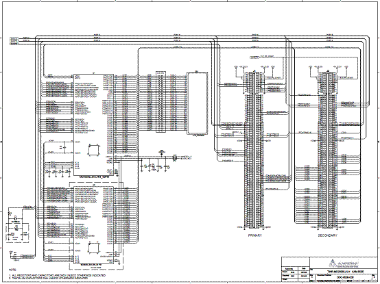
图3.演示板DEMO9S08LL16电路图(1)
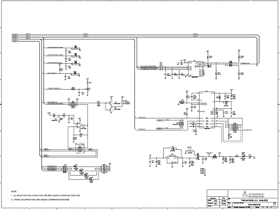
图4.演示板DEMO9S08LL16电路图(2)
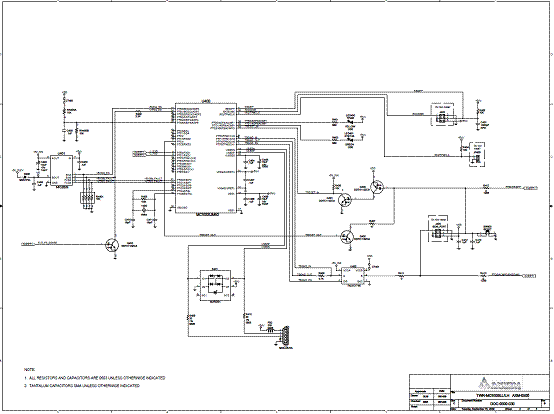
图5.演示板DEMO9S08LL16电路图(3) |
 |手机版|MCU资讯论坛
( 京ICP备18035221号-2 )|网站地图