本文包含原理图、PCB、源代码、封装库、中英文PDF等资源
您需要 登录 才可以下载或查看,没有账号?注册会员
×
Optimization of the MAX4990 High-Voage DC-AC Converter for EL Lamps
Abstract: The AC waveform (for voltage level and frequency) across an electroluminescent (EL) lamp affects brightness, current consumption, and the color of emitted light, and adjustment of the output waveform's slew rate affects the audible noise generated by the lamp itself. Consequently, the MAX4990 circuit must be optimized according to the requirements for each application. This application note provides information regarding circuit optimization and indicates the best external components to be used with the MAX4990.
IntroductionThe MAX4990 is a high-voltage DC-AC converter designed to drive electroluminescent (EL) lamps. To generate the high voltage necessary to drive an EL panel, the MAX4990 utilizes a high-frequency boost converter and a high-voltage, full-bridge output stage to generate a high-voltage AC waveform suitable for driving the EL lamp. The MAX4990's proprietary acoustic noise-reduction circuit controls the slew rate of the AC voltage driving the EL panel, thus reducing audible noise.
The MAX4990 provides a DIM pin that allows the user to set the EL output voltage through a PWM or DC analog voltage, or by connecting a resistor to GND. A capacitor placed in parallel to the resistor src="/data/attachment/portal/201007/ET33836201007230417501.gif">
Figure 1. Simplified EL lamp diagram showing its resistance and capacitance.
When alternating voltage is applied to the electrodes of an EL lamp, phosphor electrons in the outermost energy level (valance band) are energized and transition to a higher energy level. However, because the higher energy level is not stable, the excited electrons return to their original energy level, thereby releasing photons. Due to even distribution of the phosphor particles, the light emitted by an EL lamp is uniform throughout the surface of the lamp.
A change in frequency has an affect src="/data/attachment/portal/201007/ET33836201007230417502.gif">
Figure 2. Boost converter for high DC-output-voltage generation.
As switch Q is turned src="/data/attachment/portal/201007/ET33836201007230417503.gif">
Figure 3. The resistance value of the SLEW pin is used with the capacitance of the SW pin to calculate the switching frequency of LX.
The LX switching frequency can then be calculated as follows:

Driving a PWM signal directly into the SW pin, as illustrated in Figure 4.
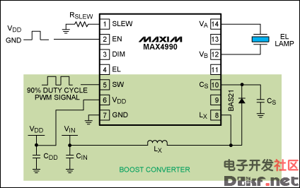
Figure 4. A 90% duty cycle PWM signal is driven into the SW pin.
The selection of the inductor is very important, as we need to make certain that the boost converter is capable of managing the application's required current level without saturating the inductor. Therefore, we must pay close attention to the inductor's current saturation level. The current through an inductor (ILX can be calculated as follows:

Where:
VIN = Inductor supply voltage
RLX = Inductor resistance
LX = Inductor value
RQ = Internal DMOS switch resistance
fSW = Inductor switching frequency
tON = (duty cycle)/fSW = Internal MOSFET switch src="/data/attachment/portal/201007/ET33836201007230417507.gif">
Figure 5. The red circle shows where a scope probe should be placed to detect inductor saturation.
Figure 6 shows how to detect when an inductor is entering saturation. The voltage at the bottom of the waveform is not rising linearly and is bent upward, indicating that the inductor is starting to saturate.
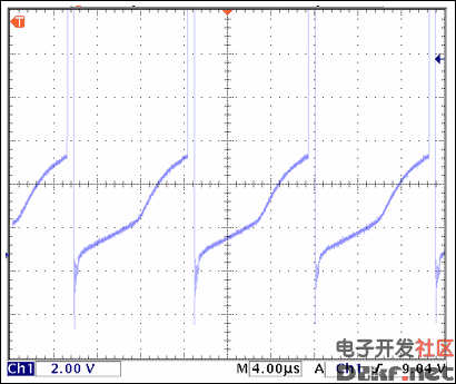
Figure 6. The inductor is starting to saturate when the waveform is bent upward instead of rising linearly.
The waveform for an inductor that is in the normal range of operation appears similar to that in Figure 7. The voltage at the bottom of the waveform is rising linearly, thus showing that the inductor is not being saturated.
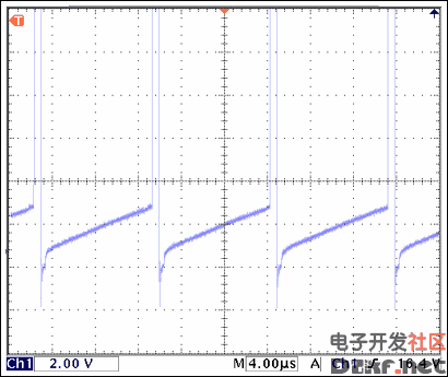
Figure 7. No inductor saturation is occurring, as evidenced by the bottom of the waveform rising linearly.
To prevent a given inductor from saturating, a shorter src="/data/attachment/portal/201007/ET338362010072304175010.gif">
Applying a clock signal to the EL pin. In this case, the fEL is ¼th of the clock frequency. Lamp brightness intensifies as frequency is increased, as illustrated in Figure 8. Keep in mind that, as the fEL is increased, a higher amount of current from a given input voltage is required to drive a given lamp size.
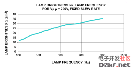
Figure 8. An EL lamp's brightness and frequency increase concurrently.
Once the fEL is selected, the peak-to-peak voltage (VP-P) across the lamp must be selected to achieve the desired brightness. The AC VP-P is controlled by:
A combination of RDIM and RSLEW, which can be calculated as follows:

A PWM signal applied to the DIM pin. The PWM signal's duty cycle is internally translated from 0 to 1.V.
A DC voltage applied to the DIM pin. Increasing the DC voltage from 0.35V to 1.3V increases the VP-P across the lamp from 70V to 250V. EL lamp brightness increases as the output voltage across the lamp is increased (see Figure 9). Applying a higher voltage across the lamp requires that a higher current is drawn from the inductor's input voltage source.
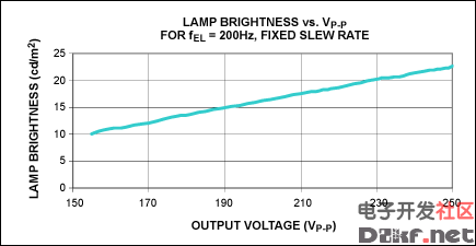
Figure 9. EL lamp brightness also increases as VP-P increases.
For applications that are sensitive to audible noise, the output waveform's slew rate is very important, as it enables the user to shape the output waveform to reduce the audible noise generated by the EL lamp.
The output waveform's slew rate is controlled through RSLEW, which is connected from the SLEW pin to GND. This slew rate can be calculated as follows:

An ideal output slew rate that minimizes audible noise generated by the lamp is dependent upon the lamp size and mechanical enclosure. Therefore, resonant frequency of the enclosure must be taken into account when selecting fEL for a given lamp size.
A sinusoidal waveform is believed to be optimal for providing the least amount of audible noise generated by the lamp. However, a sinusoidal waveform also generates less brightness than a square waveform at a given voltage level and frequency. Hence, each circuit must be optimized according to the requirements for its individual application.
As the slew rate of the output waveform is decreased, audible noise generated by the EL lamp is decreased and a lower amount of current is drawn. However, a slower slew rate does decrease lamp brightness, as seen in Figure 10.
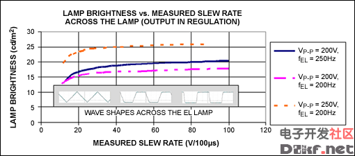
Figure 10. Lamp brightness is decreased as the slew rate slows.
To recover the brightness lost due to decreasing the slew rate, VP-P across the lamp needs to be increased. This can easily be done by increasing the desired output voltage and using a slower fSW for a given input voltage. A slower fSW increases the inductor src="/data/attachment/portal/201007/ET3383620100723041750.gif">
Figure 11. This waveform is optimal for applications sensitive to audible noise.
The MAX4990 has yet another feature that makes it even more desirable for many applications—its slow turn-on/turn-off time provides a gradual EL lamp turn-on (fade in) and turn-off (fade out).
This slow turn-on/turn-off feature is controlled by connecting a capacitor, CDIM, in parallel with RDIM to GND (Figure 12).
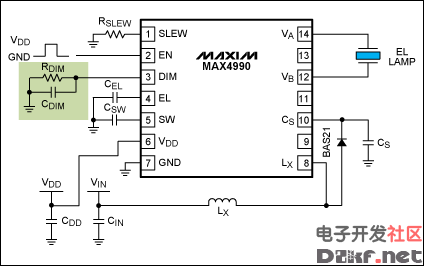
Figure 12. CDIM is connected in parallel with RDIM to GND.
The slow turn-on/turn-off time is a result of slow voltage decay across RDIM and CDIM, and it can be approximated as follows:


Figure 13 shows the affect of using CDIM in parallel with RDIM for slow turn-on/turn-off of the EL lamp.
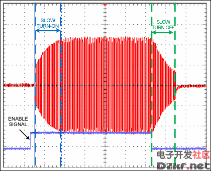
Figure 13. Slow turn-on and turn-off are shown for the MAX4990 when CDIM is connected in parallel with RDIM to GND.
Optimizing the MAX4990 CircuitTo optimize an EL lamp circuit when using the MAX4990, the following steps must be taken:
Use RSLEW = 100kΩ. RSLEW may be changed later to optimize/minimize the audible noise generated by the lamp.
Select an inductor value based src="/data/attachment/portal/201007/ET338362010072304175021.gif">
Figure 14. The MAX4990 EV kit is not in regulation.
The following was measured for VDD = 3.6V:
IDD = 26mA, brightness = 24.6cd/m2, RSLEW = 100kΩ (VR1 + R1 src="/data/attachment/portal/201007/ET338362010072304175022.gif">
Figure 15. The step time can be measured to determine fSW.
Measure the wih of a step (tSTEP) by looking at top 1/3 of either VA or VB to calculate:

Change fSW through VC1 to increase the output voltage to a level that approximately provides the desired brightness (Figure 16).
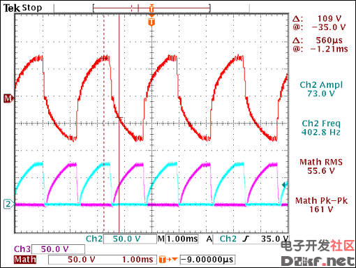
Figure 16. A sufficient brightness level has been reached.
The following was measured for VDD = 3.6V: IDD = 46mA, brightness = 35.2cd/m², RSLEW = 100kΩ, RDIM = 73.8kΩ
Check the waveform to make sure that the inductor is not saturated, as shown in Figure 17.
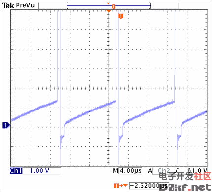
Figure 17. The waveform should show no signs of inductor saturation.
Calculate fSW as in equation 8 from step 6 (Figure 18).
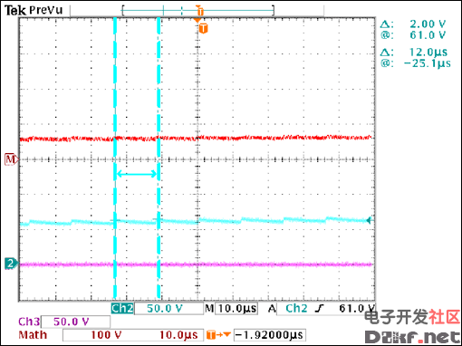
Figure 18. Measure step time to determine fSW.
For applications sensitive to audible noise, continue by repeating step 5 (Figure 19).
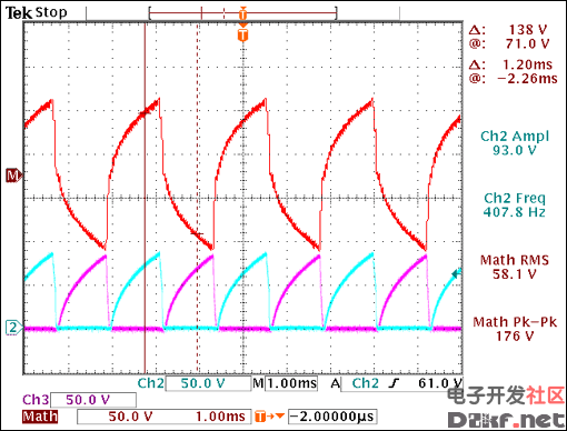
Figure 19. The waveform has no plateau, showing that the device is not in regulation.
The following was measured for VDD = 3.6V:
IDD = 53mA, brightness = 38.5cd/m², RSLEW = 100kΩ, RDIM = 87kΩ
With JU1 in positions 2 and 3, use VR1 to change the slew rate of output waveform's rising and falling edges. Note that the faster slew rate (dV/dt) provides higher brightness, but it also causes the EL lamp to generate a higher audible noise (Figure 20).
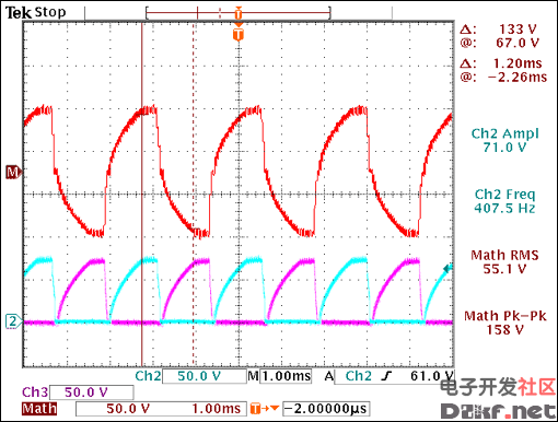
Figure 20. Slew rate adjustment.
The following was measured for VDD = 3.6V:
IDD = 45mA, brightness = 33.5cd/m², RSLEW = 120.9kΩ, RDIM = 87kΩ
Repeat step 5 to make certain the device is not in regulation (Figure 21).
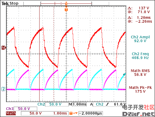
Figure 21. Again, the waveform is checked to make certain the device is not in regulation (no waveform plateau).
The following was measured for VDD = 3.6V: IDD = 52mA, brightness = 38cd/m2, RSLEW = 120.9kΩ, RDIM = 114.7kΩ
Repeat step 8 to check for inductor saturation (Figure 22).
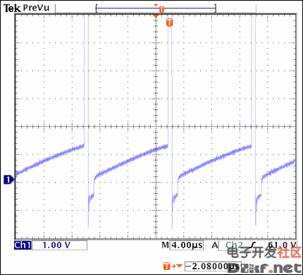
Figure 22. As can be seen from the waveform, the inductor is not saturated.
Repeat step 11 to change the slew rate (Figure 23).
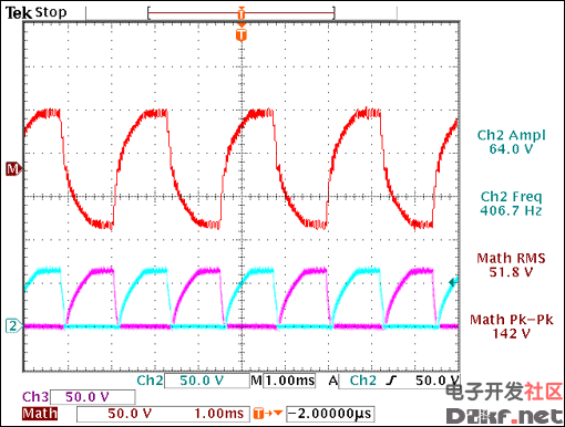
Figure 23. Slew rate adjustment is required to eliminate waveform plateau.
The following was measured for VDD = 3.6V:
IDD = 36mA, brightness = 27.7cd/m², RSLEW = 178kΩ, RDIM = 87kΩ
Repeat step 5 to make certain the device is not in regulation (Figure 24)
.
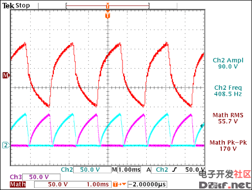
Figure 24. No plateaus at the top of the waveform indicates that the device is not in regulation.
The following was measured for VDD = 3.6V:
IDD = 49mA, brightness = 36.9cd/m², RSLEW = 178kΩ, RDIM = 181.8kΩ
Repeat steps 7, 8, 9, 11 and 5 (in this order) until you achieve the desired brightness with the appropriate waveform shape for your application (Figures 25 and 26).
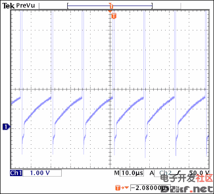
Figure 25. Step 8 is repeated to check for inductor saturation.
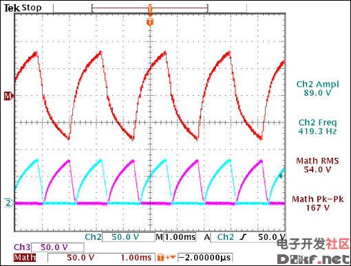
Figure 26. Repeating step 5 shows that the device is not in regulation.
The following was measured for VDD = 3.6V:
IDD = 56mA, brightness = 37.5cd/m², RSLEW = 260.5kΩ, RDIM = 239.4kΩ
Calculate fSW using equation 8 from step 6 (Figure 27).
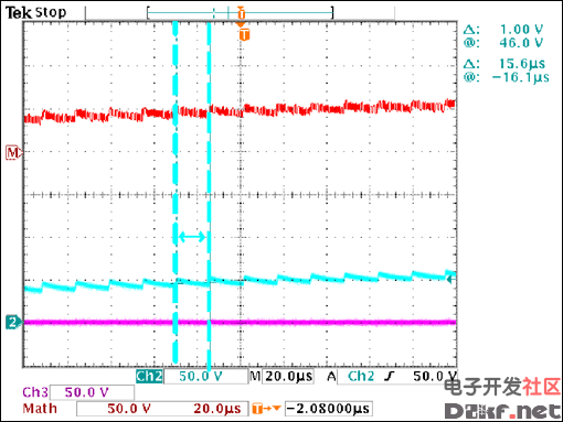
Figure 27. As in step 6, step time can be measured to determine fSW.
Using equation 8:

Measure the RDIM and RSLEW values.
RDIM = 239.4kΩ
RSLEW = 260.5kΩ
Note that the RSLEW value would be the value>

Select the closest available capacitor values to the values calculated for your circuit. Some minor adjustments to RSLEW and RDIM may be required based src="/data/attachment/portal/201007/ET338362010072304175038.gif">
<-- END: DB HTML --> |
|
 |手机版|MCU资讯论坛
( 京ICP备18035221号-2 )|网站地图