本文包含原理图、PCB、源代码、封装库、中英文PDF等资源
您需要 登录 才可以下载或查看,没有账号?注册会员
×
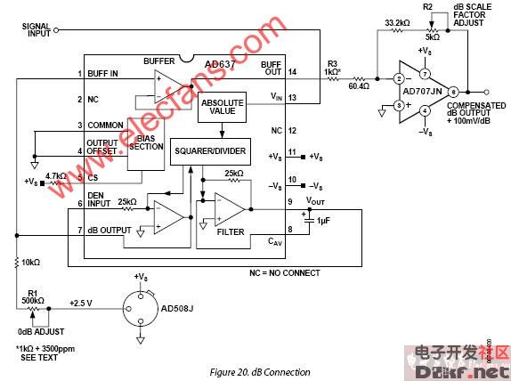
ad637应用电路

dB CALIBRATION
Refer to Figure 20:
? Set V
= 1.00 V dc or 1.00 V rms IN
? Adjust R1 for 0 dB out = 0.00 V
? Set V = 0.1 V dc or 0.10 V rms IN
? Adjust R2 for dB out = ?2.00 VAny other dB reference can be used by setting VIN and R1 accordingly.The AD637 is a complete, high accuracy, monolithic rms-to-dc converter that computes the true rms value of any complex waveform. It offers performance that is unprecedented in integrated circuit rms-to-dc converters and comparable to discrete and modular techniques in accuracy, bandwidth, and dynamic range. A crest factor compensation scheme in the AD637 permits measurements of signals with crest factors of up to 10 with less than 1% additional error. The wide band-width of the AD637 permits the measurement of signals up to 600 kHz with inputs of 200 mV rms and up to 8 MHz when the input levels are above 1 V rms.
As with previous monolithic rms converters from Analog Devices, Inc., the AD637 has an auxiliary dB output available to users. The logarithm of the rms output signal is brought out to a separate pin, allowing direct dB measurement with a useful range of 60 dB. An externally programmed reference current allows the user to select the 0 dB reference voltage to correspond to any level between 0.1 V and 2.0 V rms. |
|
 |手机版|MCU资讯论坛
( 京ICP备18035221号-2 )|网站地图