本文包含原理图、PCB、源代码、封装库、中英文PDF等资源
您需要 登录 才可以下载或查看,没有账号?注册会员
×
TI公司的TPS51650和TPS59650是集成了两个栅极驱动器的双路 VID全兼容的IMVP-7降压控制器,支持CPU和GPU输出,CPU通路具有一相,二相或三相,GPU通路具有一相或二相,8位 AC具有0.250V到1.52V的输出,转换电压范围3V到28V,主要用在IMVP-7 VCORE以及适配器,电池,NVDC或3V,5V和12V电源.本文介绍了TPS51650和TPS59650主要特性,方框图,多种典型应用电路,以及TPS59650EVM-753评估模块主要特性和指标,方框图,电路,材料清单和PCB元件布局图.
The TPS51650 and TPS59650 are dual-channel, fully SVID compliant IMVP-7 step-down controllers with two integrated gate drivers. Advanced control features such as D-CAP+ architecture with overlapping pulse support (undershoot reduction, USR) and overshoot reduction (OSR) provide fast transient response, lowest output capacitance and high efficiency. All of these controllers also support single-phase operation for light loads. The full compliment of IMVP-7 I/O is integrated into the controllers including dual PGOOD signals, ALERT and VR_HOT. Adjustable control of VCORE slew rate and voltage positioning round out the IMVP-7 features. In addition, the controllers’ CPU channel includes two high-current FET gate drivers to drive high-side and low-side N-channel FETs with exceptionally high speed and low switching loss.
TPS51650和TPS59650主要特性:
Intel IMVP-7 Serial VID (SVID) Compliant
Supports CPU and GPU Outputs
CPU Channel One-Phase, Two-Phase, or Three-Phase
One-Phase or Two-Phase GPU Channel
Full IMVP-7 Mobile Feature Set Including Digital Current Monitor
8-Bit DAC with 0.250-V to 1.52-V Output Range
Optimized Efficiency at Light and Heavy Loads
VCORE Overshoot Reduction (OSR)
VCORE Undershoot Reduction (USR)
Accurate, Adjustable Voltage Positioning
8 Independent Frequency Selections per Channel (CPU/GPU
Patent Pending AutoBalance™ Phase Balancing
Selectable 8-Level Current Limit
3-V to 28-V Conversion Voltage Range
Two Integrated Fast FET Drivers w/Integrated Boost FET
Selectable Address (TPS59650 only)
Small 6 × 6 , 48-Pin, QFN, PowerPAD Package
TPS51650和TPS59650应用:
IMVP-7 VCORE Applications for Adapter, Battery, NVDC or 3-V, 5-V, and 12-V Rails
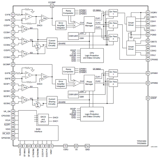
图1.TPS51650和TPS59650方框图
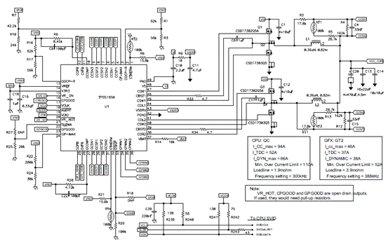
图2.TPS51650带电感DCR电流检测的三相CPU,2相GPU应用电路图
图3.带电感DCR电流检测的一相GPU应用电路图

图4.带电感DCR电流检测的三相CPU应用电路图

图5.带电感DCR电流检测的2相CPU应用电路图
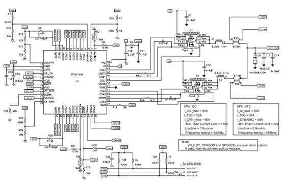
图6.带电感DCR电流检测的2相CPU和GPU不能的应用电路图
TPS59650EVM-753评估模块
The TPS59650EVM-753 is designed to use a 9V-20V Input bus to produce 6 regulated outputs for IMVP7 SVID CPU/GPU Power System. The TPS59650EVM-753 is specially designed to demonstrate the TPS59650 full IMVP7 mobile feature while providing GUI communication programing and a number of test points to evaluate the static and dynamic performance of TPS59650.
TPS59650EVM-753评估模块典型应用:
· IMVP7 Vcore Applications for Adapter, Battery, NVDC or 3V/5V/12V rails
TPS59650EVM-753评估模块主要特性:
· Complete solution for 9V-20V Input Intel IMVP7 SVID Power System
· GUI communication to demonstrate full IMVP7 Mobile feature
· 3-Phase CPU Vcore can support up to 94A output current
· 2-Phase GPU Vcore can support up to 46A output current
· 8 Selectable Switching frequency for CPU and GPU power
· 8 Levels selectable current limit for CPU and GPU power
· Switches or Jumpers for each output enable
· On Board Dynamic Load for CPU, GPU Vcore and VCCIO output
· High efficiency and high density by using TI power block MOSFET
· Convenient test points for probing critical waveforms
· Eight Layer PCB with 1oz copper SLUU896–
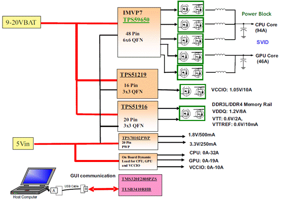
图8.TPS59650EVM-753电源系统框图
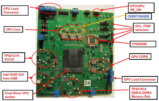
图9.TPS59650EVM-753外形图
TPS59650EVM-753电性能指标:
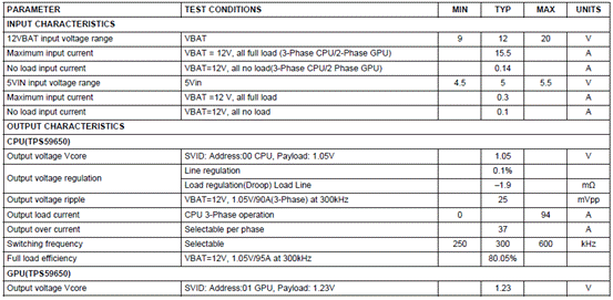
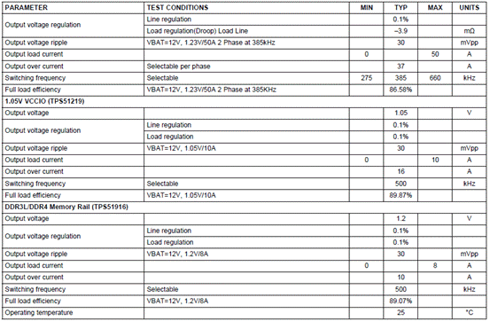
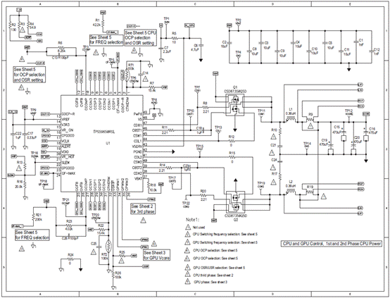
图10.TPS59650EVM-753电路图(1)
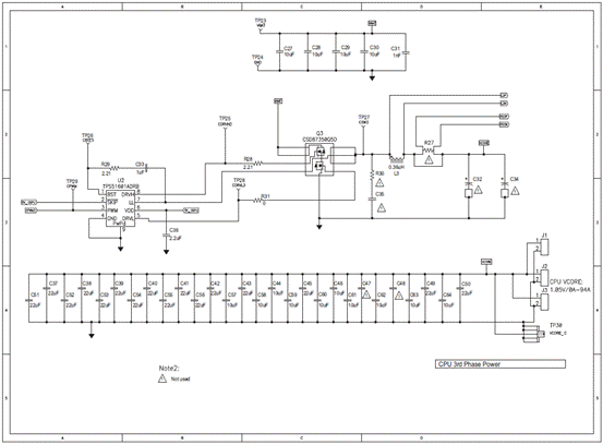
图11.TPS59650EVM-753电路图(2)
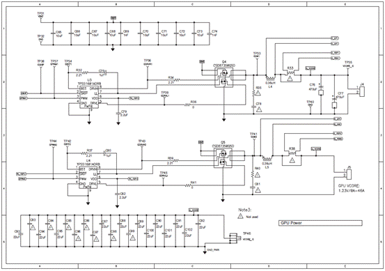
图12.TPS59650EVM-753电路图(3)
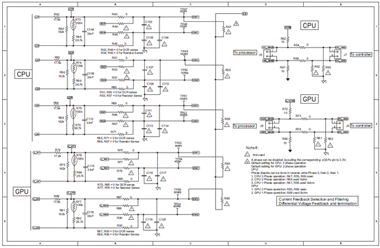
图13.TPS59650EVM-753电路图(4)
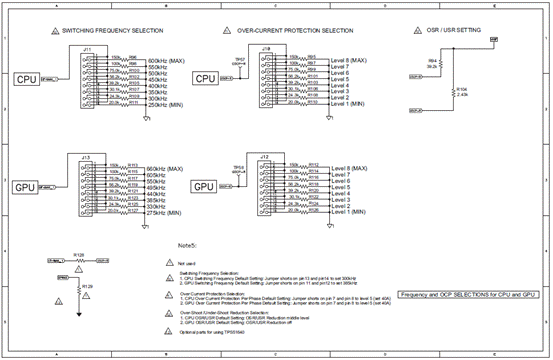
图14.TPS59650EVM-753电路图(5)
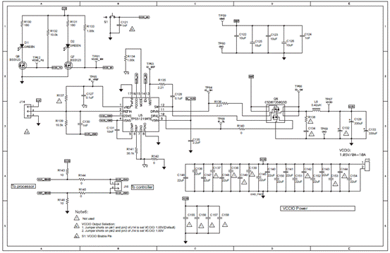
图15.TPS59650EVM-753电路图(6)
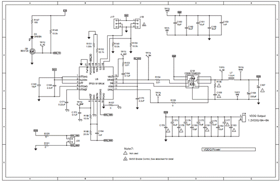
图16.TPS59650EVM-753电路图(7)
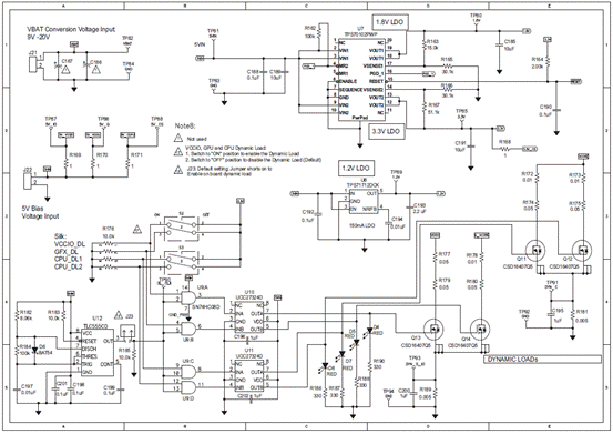
图17.TPS59650EVM-753电路图(8)
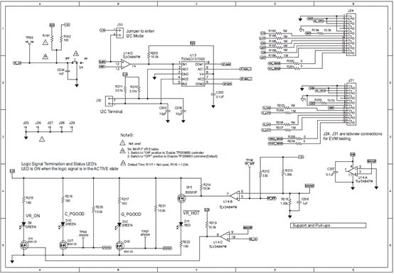
图18.TPS59650EVM-753电路图(9)
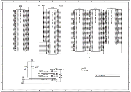
图19.TPS59650EVM-753电路图(10)
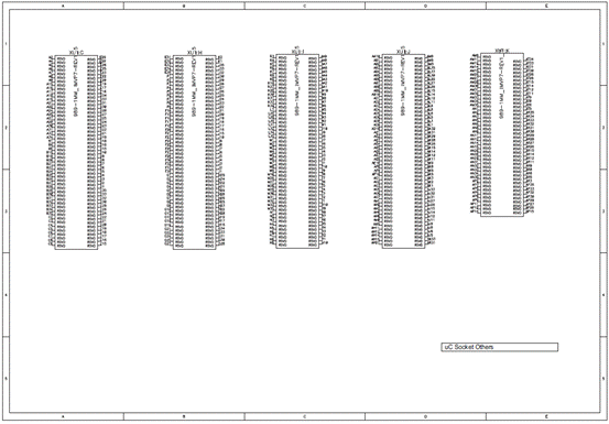
图20.TPS59650EVM-753电路图(11)
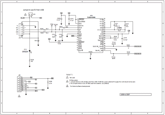
图21.TPS59650EVM-753电路图(12)
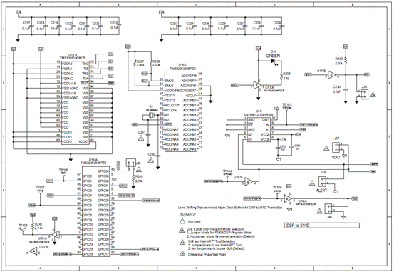
图22.TPS59650EVM-753电路图(13)
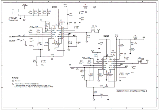
图23.TPS59650EVM-753电路图(14)
TPS59650EVM-753材料清单:
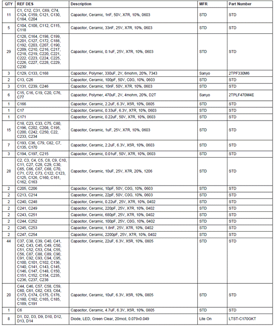
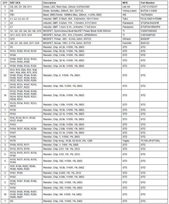
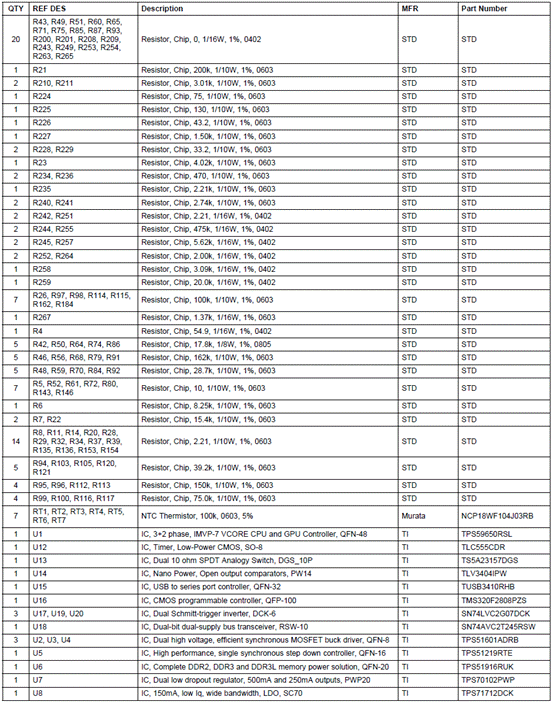

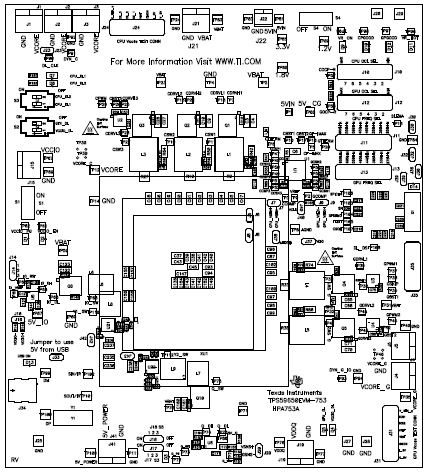
图24.TPS59650EVM-753 PCB元件布局图:顶层
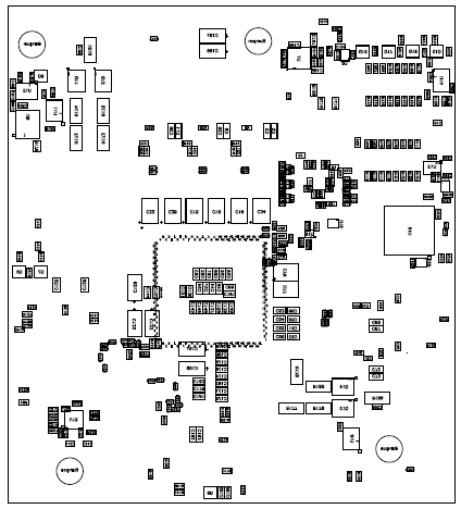
图24.TPS59650EVM-753 PCB元件布局图:底层
详情请见:
http://www.ti.com/lit/ds/slusav7/slusav7.pdf
和
http://www.ti.com/lit/ug/sluu896/sluu896.pdf |
 |手机版|MCU资讯论坛
( 京ICP备18035221号-2 )|网站地图